|
Cryptome DVDs are offered by Cryptome. Donate $25 for two DVDs of the Cryptome 12-years collection of 46,000 files from June 1996 to June 2008 (~6.7 GB). Click Paypal or mail check/MO made out to John Young, 251 West 89th Street, New York, NY 10024. The collection includes all files of cryptome.org, jya.com, cartome.org, eyeball-series.org and iraq-kill-maim.org, and 23,000 (updated) pages of counter-intelligence dossiers declassified by the US Army Information and Security Command, dating from 1945 to 1985.The DVDs will be sent anywhere worldwide without extra cost. | |||
8 May 1998
High-performance Computing, National Security Applications,
and
Export Control Policy at the Close of the 20th Century
18
Overview of Key Industry Trends
What will be the impact of industry trends on the export control regime? To understand which factors are most significant, we must understand what kinds of changes have the greatest impact on the analysis framework used to determine viable control thresholds. The framework seeks to identify performance levels that are above uncontrollable performance levels and below the performance required for key applications of national security concern. Consequently, the greatest impact on the selection of a viable control threshold comes from factors that impact
1. the lower bound of controllability, and
2. the application of high-performance computing technologies to problems of national security concern.
Of particular interest are trends that make it possible to pursue important applications using hardware and software platforms that are considered uncontrollable.
In this chapter, we examine the factors that most strongly impact these two aspects of the framework. Other factors will be covered in greater depth in subsequent chapters. The factors discussed here are
1. Performance. A primary factor driving the threshold of controllability upward over time is the improved performance of products occupying a given market/price niche. Since the composite theoretical performance is a processor-oriented metric, we focus our attention on developments in processors. However, realizable performance of systems is also a function of the speed of memory, interconnects, I/O, and systems software. We briefly touch on these factors as well.
2. Scalability and the ability to harness the computing power of multiple, smaller systems. As we 'discuss at greater length in the next chapter, the ability to increase the performance of a system incrementally, or to combine the resources of multiple, independent systems into a computing cluster has a significant impact on the performance that can be attained through straightforward combinations of uncontrollable platforms. We identify industry advances in interconnects and systems software that make it easier to combine systems or to extend the performance of existing systems.
Recent Trends in Processor Performance and Capability
There can be no doubt that advances in microprocessor technologies are the dominant forces shaping the export control regime today. This is true for at least three reasons. First, the performance of microprocessors is increasing rapidly. All other factors being equal, the threshold of controllability rides this curve, since all uncontrollable platforms today are based on microprocessor technology. Second, microprocessors and other technologies traditionally associated with workstation markets are today being used by all HPC vendors from the low-end
19
desktop uniprocessors to the most powerful massively parallel systems Third, microprocessors are the most straightforward and uncontroversial contributors to CTP.
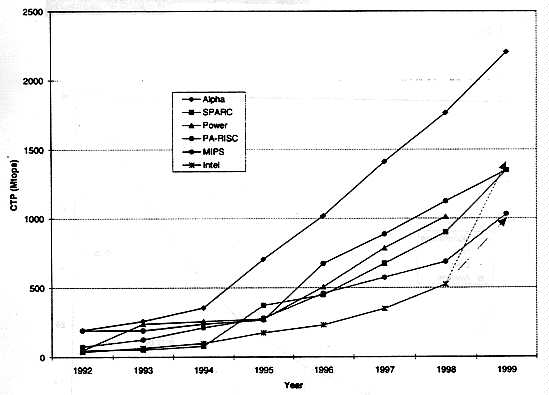
Figure 4 illustrates the dramatic improvements in microprocessor performance since 1992 All of the data represent microprocessors in volume production; systems based on the microprocessors are generally available from vendors. The chart indicates that by 1997, nearly all of the major RISC/UNIX workstation vendors were incorporating processors above 500 Mtops into their products. The figures for 1999 are estimates, based on publicly available data Since vendors often introduce microprocessors at clock speeds slightly different from what had been announced, actual figures might vary slightly. Intel processors in volume production will lie somewhere in the range indicated by the two Intel arrows.
Figure 4 Performance of microprocessors in volume production.
The improvements in microprocessor performance have been driven primarily by advances in process technologies and in microprocessor architectures. Advances in process technologies have led to smaller feature sizes and greater numbers of transistors per microprocessor. These developments have permitted more functional units, control logic, and cache to be placed in a given amount of space. Carefully designed architectures have permitted the clock rates to increase. Since the number (and type) of instructions issued and the clock rate are two of the most significant parameters in the calculation of the CTP, these factors have been at the heart of the performance increase. Figure 5 and Figure 6 illustrate how feature sizes have shrunk, and transistor counts have grown since 1992.
20
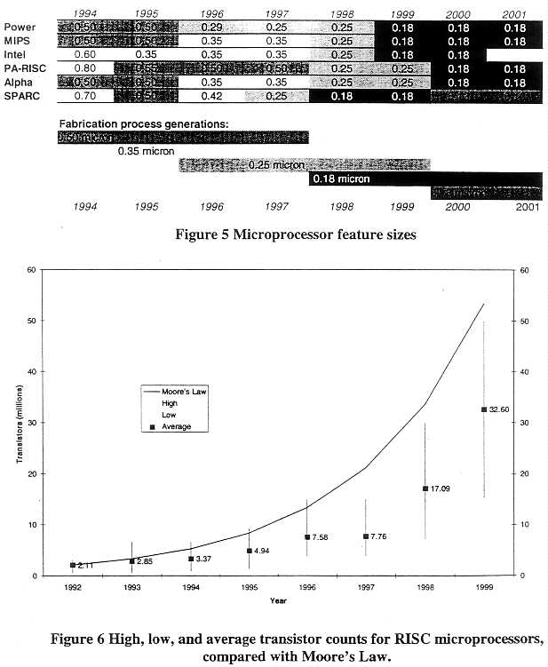
Figure 7 and Figure 8 show how clock frequencies and instruction issue rates have increased during the same period. The slight drop in the average clock frequency during 1995 reflects the fact that MIPS technologies introduced in that year the R8000 at 75 MHz, a processor with more power but a slower clock than its predecessor, the R4400 (250 MHz). The slower clock was
21
necessary because the R8000 processor was a dual-chip processor whose signals needed extra time to propagate from one chip to the other.
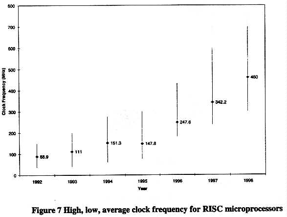
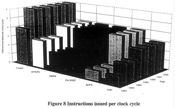
Figure 8 illustrates that sustained issue rates of four instructions per clock cycle is the standard throughout most of the industry. The jump to higher instruction issue rates by most of the microprocessor vendors, combined with the increases in clock speed enabled by process improvements, accounts for the sharp increase in processor performance in 1994-1996 shown in Figure 4. The next sharp increase in issue rates is projected to come in 1999-2000.
22
Future Microprocessor Developments and Challenges
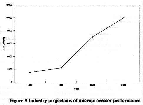
Over the next 3-4 years, microprocessor performance measured in CTP is likely to grow dramatically. Figure 9 shows some industry projections--representing no single vendor--for processor performance over the next several years.
23
The growth in performance is fueled by a combination of factors, including
Process technologies
Moore' s Law states that the number of transistors on a chip will double approximately every l8 months. The data in Figure 6 show that the average number of transistors used in processors has not increased this rapidly during the last few years. However, if industry predictions are correct, transistor counts will "catch up" in the near future reaching on the order of 50 million transistors by 1999 [1]. The roadmaps for photolithography indicate that current trends will continue until at least 2003-2004. Vendors are now counting on feature sizes of 0.18 microns by the early part of the 21st century. Current technological approaches may be able to reduce feature size to one more generation, or 0. 13 microns [2]. Beyond this point, feature size will be less than the wavelength of the ultraviolet light (UV) used in lithography today, and the industry will have to move to light with smaller wavelengths, such as X-ray. It is still unclear how smooth the transition to post-UV lithography will be. Historically, the semiconductor industry has shown a remarkable ability to continue a breathtaking rate of technological advance over decades. Eventually the fundamental laws of physics will halt the trends towards smaller feature sizes, but it is not at all clear that this will be within the next ten years.
24
As feature size shrinks and gate delays decrease, reducing the cycle time has been a popular and relatively easy way of increasing performance Figure 6 shows that between 1992 and 1997 the average clock frequency increased by nearly 400%, substantially more than the 160% improvement many microprocessor designers had predicted over these five years [3] Unfortunately, as feature size drops below 0 25 microns and clock frequencies increase, signals are no longer able to propagate across the entire die. In addition, the signal delays within individual wires increase as the wires become thinner. In [2], Doug Matzke calculates that in a microprocessor with 0.1 micron feature size and a 12 GHz clock, only 16 percent of the die is reachable within a clock period. Industry is recognizing these limitations. The Semiconductor Industry Association (SIA) projects that in 2012, clock rates will be about 2.7 GHz, nearly an order of magnitude less than if the trends of the last five years were to continue for the next fifteen [4].
Microprocessor architectures
If we suppose that trends in shrinking feature size continue, microprocessors manufactured using 0.1 8 micron technology are likely to have up to 50 million transistors in 1999-2000, and a hundred million or more in 2001-2004. The SIA has predicted that by 2007 the number of transistors will reach 350 million, and 800 million by 2010 [5]. A more recent SIA roadmap indicates that microprocessors will have 1.4 billion transistors by 2012, provided a number of fundamental fabrication problems are solved [4]. A crucial question for microprocessor architects is how to best use this abundance? For the export control regime, an important question is what impact the new architectures are likely to have on performance.
A number of leading researchers are considering how a billion transistors would be used [6-11]. Although there is considerable variety (and lack of consensus) in the specific techniques being taken to solve this problem, there are three principal strategies employed [8]:
A single-chip multiprocessor is based on two main observations: a) It is becoming increasingly difficult to extract parallelism from a single thread of execution. To do so requires a disproportionate amount of chip real estate devoted to instruction scheduling, branch prediction, and so forth. b) The problems of wire delays on chips with features under 0.25 microns will force designers to create partitioned chips with highly localized functionality within each partition. The benefits of a single-chip multiprocessor are that it is inherently partitioned, and is fundamentally designed to accommodate multiple threads of execution, greatly increasing the amount of parallelism that can be exploited. In a system proposed in [10], a single chip consists of eight CPUs which share 8 Mbytes of secondary cache. Each CPU can issue two instructions per cycle. If a single-chip multiprocessor with these characteristics were implemented with a 2
25
GHz clock, it would have approximately 16 times the performance (4x instruction issue and 4x clock) of a typical 1997 microprocessor. Depending on the year in which it is manufactured, the processor would represent a doubling of processor performance every two or three years.
A second approach is typified by the Berkeley V-IRAM project [9]. In this design, most of the on-chip memory is occupied not by static RAM (SRAM) caches whose contents are understood to be copies of instructions and data stored in main memory, but by dynamic RAM (DRAM) which is treated as main memory. In one proposed layout, DRAM would occupy 99% of the transistors (800 million), while the CPU and caches would occupy just 3 million and the vector unit would occupy 4 million. The vector unit would have two arithmetic units, each capable of producing eight results per clock. With the 1 GHz clock proposed by the developers, this processor would likely have a CTP approximately eight times today's microprocessors, or on the order of 6000 Mtops. An implementation would require 0.13 micron technology, which could be feasible in the years 2002-2004. The performance gain of such a processor would represent, on the average, a doubling of microprocessor performance every two years from 1998 through 2004.
The third approach employs a large uniprocessor using 24 to 48 highly optimized, pipelined functional units. The goal to place on a single chip those elements that must be close together in order to minimize latency, and to minimize data traffic to off-chip locations. The functional units, instruction issue logic, and extensive cache memory are placed on-chip, while main memory, I/O, and other processors are located off chip. A key challenge under such circumstances is enabling the processor to issue and usefully execute 16 to 32 instructions each clock cycle without overwhelming the off-chip memory bandwidth. In a design proposed by Patt et al [7], the challenges are addressed by devoting nearly 90% of the transistors to various kinds of caches, with only about 10% to logic (6% for the execution core itself). By comparison, logic occupies nearly 40% of the transistors in the MIPS R10000 and just over 50% in the Alpha 21164. Assuming a 2 GHz clock in the year 2010, a large uniprocessor is likely to have 16 to 32 times the (theoretical) performance of the typical 700 Mtops processor of 1997, or 11K to 22K Mtops. This represents a doubling of performance every three years.
In each of the approaches discussed above, increasing the number of instructions issued and executed per clock period, and shortening the clock period increases theoretical performance. The principal differences lie in areas that have no great impact on the CTP as currently formulated. While the CTP is a function of the number and types of computational elements, the clock period, and the word-length, the approaches outlined above differ from each other mostly in the techniques used to keep the functional units occupied and to contain design complexity, programming complexity, or both. Scheduling and issue logic and caches play a critical role in delivering real performance, but do not contribute to the performance measured by the CTP.
Will the delivered performance of tomorrow's microprocessors grow faster, slower, or at the same rate as the CTP? The question cannot, of course, be settled until chips are manufactured and tested. Chip designers will certainly devote a disproportionate amount of chip real estate to memory, cache, and administrative functions. If designers are very successful in these efforts, better use may be made of each execution unit than has been the case in the past, and the
26
deliverable performance will increase faster than the CTP In other words, while the CTP may grow by a factor of 16 to 32, the observable performance on real applications may grow more quickly It is not, however, a foregone conclusion that such efforts will be successful.
Chip designers face enormous challenges in keeping functional units occupied The current state of the art has difficulty keeping four, let alone six functional units busy. Microprocessors such as the DEC 21264, the MIPS R10000, and the PowerPC 604 typically achieve only about 0.5 to 1.5 sustained instructions per cycle (out of a potential of four per cycle) on real-world problems [12] Part of the problem is that functional units spend most of their time waiting for instructions or data. The other part of the problem is that functional units today are pipelined, meaning that at any point in time there may be from 5-12 instructions at various stages of execution. The processor must fetch the next instruction before the current one has finished executing. In portions of code involving conditional statements (IF-THEN) the "next" instruction is dependent on the result of a current calculation. The processor must guess which instruction will be next; if it guesses wrong, the pipeline will stall until the correct instructions can be fetched. This penalty may be a wait of several cycles, dramatically reducing utilization. If the potential number of instruction issues per clock period increases to six or sixteen, the task of keeping all, or even a comparable fraction, of the functional units busy increases substantially.
At the same time, increasing clock frequencies makes the penalty for missing a needed instruction or data element greater. For example, if the CPU clock runs at 400 MHz, a 2.5 nanosecond (nsec) clock period, but main memory access time is 60 nsec, then the time a functional unit must wait for a data element is 24 CPU cycles. The cost in utilization of that functional unit is enormous. The difficulty lies in the fact that the gap between the speed of the CPU and the speed of main memory is widening, not shrinking or even holding constant. At the same time, the presence of growing numbers of functional units will require the volume of data flowing across chip pins to grow correspondingly. The challenges are so formidable that Richard Sites, a senior architect at Digital Equipment Corporation, has stated, "over the coming decade memory subsystem design will be the only important design issue for microprocessors" [3].
Impact of emerging applications
The cost of microprocessor fabrication is enormous, and increasing. In 1993, a 0.8 micron facility cost approximately $200-300 million to build and mature [13]. Today, new fabrication plants, which must be built for new generations of process technology, cost $1-2 billion each [14,15]. In five or ten years, the cost could rise to $4 billion [4]. This cost must be recovered in a very few years, before the next fabrication plant is built. The only way to recover these costs is to sell hundreds of thousands of high-priced processors, or millions of low-priced ones. The only way to sell large volumes of microprocessors is to design them to serve the mass markets of desktop, embedded, or entertainment systems.
What applications will drive microprocessor design, and what are the implications of the new designs for CTP performance? There is broad agreement that multimedia and user interface workloads will consume a growing proportion of a microprocessor's processing power. Multimedia intensive applications include animation, video-conferencing, visualization, image
27
processing, realistic simulation, and so forth Nearly all CPUs introduced in recent years contain features for improved multi-media performance. Table I shows measures taken by various vendors to support multimedia workloads.
| Processor family | Multimedia capability |
| Intel | Multimedia Extension (MMX) |
| Alpha | Motion-video instructions (MVI) |
| MIPS | MIPS digital media extensions (MDMX) |
| SPARC | Visual Instruction Set (VIS) |
| PA-RISC | MAX2 |
Table 1 Multimedia support in major microprocessor families
Multimedia applications have a number of characteristics that distinguish them from traditional workloads. These include [16]:
The approach taken in one fashion or another by most microprocessor vendors to date has been the addition of specialized multimedia instructions to the existing instruction set. A common technique (MIPS, Intel, SPARC) is to use existing floating-point registers to process not just one (64-bit) data element at a time, but multiple 8- or 16-bit data elements that have been packed into a 64-bit word. The techniques used on the Alpha and PA-RISC chips utilize integer registers for the same purpose. The extended instructions perform a variety of tasks, including packing and unpacking pixels into words, performing arithmetic and logic operations on pixels, and so forth [17- 19].
So far, the impact of multimedia extensions on CTP has been minimal. The extended instruction sets have not fundamentally changed the computational elements in a chip; they have only changed the use to which these elements have been put. If chip designers decide to create graphics units in addition to the set of more traditional fixed- and floating-point units, the CTP could correspondingly increase. By applying the same instructions on multiple pixels or audio
28
samples, these units can look a great deal like small vector units. The addition of such units could push single microprocessor CTP levels over 10,000 Mtops by the year 2002.
Significance of Microprocessor Developments for HPC
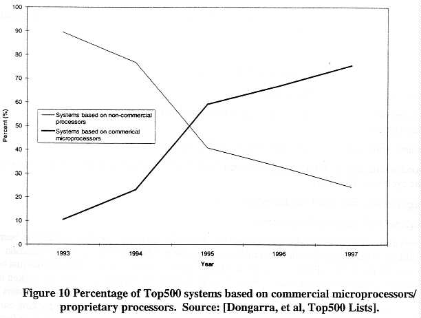
The significance of microprocessor developments for high-performance computing systems is very easily stated. By far the majority of high-performance computing systems today employ commercially available microprocessors as their compute engines. The percentage of the world's 500 most powerful computing installations employing commercially available microprocessors has grown from approximately 10% in 1993 to 75% in 1997. Figure 10 illustrates this trend clearly.
Most high-performance computing systems today are built using commercial microprocessor technologies largely for economic reasons. The price/performance of commercial microprocessor-based systems is compelling for large segments of the HPC market. For example, Figure 11 shows the price per Mtops of models introduced during 1997 by various vendors. The prices are based on advertised vendor list prices at the time of introduction. (The C90, introduced in 1991 is provided for additional comparison.) The Cray J90 does not use
29
commercial microprocessors, but does use CMOS components manufactured using processes comparable to those used by the leading microprocessor vendors.
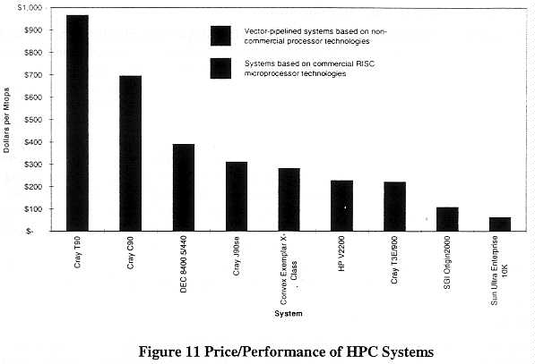
The figure illustrates the price/performance advantage that systems based on CMOS technologies in general, and commercial CMOS microprocessors in particular, enjoy over traditional vector-pipelined systems that do not employ these technologies.
Gluing the Pieces Top,ether: Recent Trends in Systems Architecture and Capability
If systems from the low end to the high end of all HPC companies' products lines are being constructed from the same underlying microprocessor components, then computational performance as measured by the CTP will ride the rising tide of microprocessor performance. But what industry trends are shaping vendor and practitioner abilities to harness the power of aggregations of microprocessors and apply it in a concentrated fashion to real-world applications? The advances that provide the "glue" include:
1. microprocessor design features to support multiprocessing
2. interconnect and memory subsystem improvements
3. systems software advances
30
Microprocessor support of multiprocessing
While providing greater uniprocessor performance has been a constant goal of microprocessor designers, the need to build into the microprocessor itself elements that will facilitate the creation of multiprocessor systems is of growing importance.
A leading example of this trend is Sun Microsystems UltraSPARC-III, introduced in 1997 and scheduled for sampling in 1998 [20,21]. Designers decided to forego maximizing performance in favor of features that enable the CPU to function more effectively in a multiprocessor environment One measure being taken is to reduce a CPU's contention with other CPUs for shared resources A dominant architecture in the mid- 1 990s for mid-range HPC systems has been the symmetrical multiprocessor (SMP) architecture in which all CPUs have shared and uniform access to all of main memory. Local, cache memory is considered just a copy of main memory. While providing a very convenient programming and operating model, SMP systems have often suffered performance degradation in large configurations due to contention among the CPUs for memory and memory access busses. In the UltraSPARC-m, each CPU has its own main memory, which limits CPU contention to times when one CPU must access the memory of another. The logic not only for cache access but also for main memory access is migrated onto the microprocessor itself. A second set of multiprocessor-oriented design features of the UltraSPARC-m tries to minimize the impact of delays in accessing off-chip memory. These features include extensive speculative execution and non-stalling execution pipelines.
Interconnect and memory subsystems
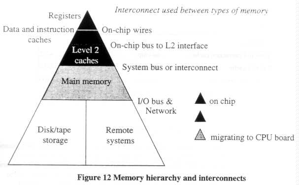
Supplying the CPUs with an adequate volume of data and instructions in a timely fashion is fundamental to system performance. In an ideal world, all memory would be accessible quickly, available in large volumes, and very cheap. The reality is that these three quantities cannot all be optimized simultaneously. The fastest memory, used in on-chip registers and caches, is available in small quantities at high cost. The cheapest memory, available as disk or tape storage, is available in large volumes, but is very slow. Second level cache and main memory have intermediate qualities. Providing large memory spaces with high bandwidth and low latency is extremely expensive, and one of the reasons traditional supercomputers have million-dollar-plus prices. Because of the price, performance, and volume characteristics of different kinds of memory, computing systems at all performance levels have adopted elaborate hierarchical memory structures that integrate different kinds of memories in varying volumes. Figure 12 illustrates the types of memory and the types of interconnect used to move data from one to the other.
31
Since the execution units of microprocessors are designed to operate only on data located in the registers, managing memory involves a complex process of moving data elements and instructions up and down this hierarchy so that the right data elements and instructions are in the registers at the right time. A system's ability to carry out this process effectively is vitally dependent on the memory management logic, and the bandwidth and latency of the memory and interconnect subsystems.
Designing the memory system is one of the great challenges of system architecture today. As microprocessor clock frequencies and the number of instructions issued per cycle increase, the system becomes increasingly sensitive to failures of the memory system to deliver the right data element to the functional units at the right time. In the event of such a failure, the CPU may have to wait until the appropriate data element or instruction is fetched from wherever it might be in the memory hierarchy and placed in the registers. In the past, accessing data in main memory required a single clock cycle. This is no longer true. Table 2 shows the typical latency, measured in clock cycles, to fetch a data element or instruction from various locations in memory. Due to the penalty incurred by a memory access "miss," designers have made enormous efforts to migrate the data and instructions most likely to be needed in the near future closer to the CPU.
32
| Type of memory |
Location |
Access time (cycles) |
| Registers | on-chip | 1 |
| Data and instruction cache | on-chip | ~1-2 |
| Level 2 cache | off-chip | ~6-10 |
| Local main memory | off-board | ~60-100 |
| Remote main memory | off-board | ~100-200+ |
| Secondary storage, networked systems |
on-disk, on-network | ~1000s-10000s+ |
Table 2 Memory latency
Under the current CTP formulation, memory subsystem characteristics affect Mtops performance in only two ways. First, in systems with logically shared main memory the contribution of multiple CPUs is weighted more heavily than in systems with logically distributed main memory Second, CPUs linked together by traditional networking technologies do not contribute to the CTP of the system. Consequently, most of the developments in memory and interconnect systems are likely to have only minimal impact on the CTP, even though they may have substantial impact on real-world performance. From the perspective of the CTP, the most significant memory and interconnect advances are those that will enable larger numbers of processing elements to be combined effectively into single systems. Of principal interest are
1. advances in system busses that accommodate greater numbers of CPUs
2. the trend away from shared system buses to switched interconnects
3. the growing use of networking or clustering interconnects with performance substantially better than traditional networks.
In 1995, Intel publicized widely that its forthcoming Pentium Pro (P6) processor was to be designed for parallel processing. One of the principal advances was the creation of a new 64-bit system bus optimized for high-bandwidth access to main memory by up to four CPUs [22]. This form of on-board multiprocessing has become quite widespread, enabling many other equipment manufacturers (OEM) such as Compaq and Dell the ability to sell multiprocessors without having to invest heavily in multiprocessing technologies of their own.
Intel, however, was a latecomer to the world of symmetrical multiprocessing, especially multi board multiprocessing. Since the late 1980s and early 1990s vendors such as Silicon Graphics, Sun Microsystems and Digital Equipment Corporation have been marketing products employing multiple processors accessing memory through a single, shared bus. To accommodate processor counts as high as 36 (in the case of Silicon Graphics Challenge servers), these vendors used busses that were hundreds of bits wide and had high bandwidth and modest latency.
Because the bus is a shared medium, however, the greater the number of processors, the less bandwidth is available. on average, for individual processors and the greater the likelihood of
33
CPUs encountering contention for the system bus. For this reason. systems could not scale beyond a modest number of processors. In practice, systems with more than 8-12 processors suffered substantial performance degradation.
HPC systems designed to accommodate large numbers of processors were designed from the start to avoid the bottlenecks of shared interconnects. Cray's T3D and T3E, IBM's SP2. Intel's Paragon, and others employed switched, or crossbar interconnects that would scale with the number of processors so that the interconnect bandwidth available per processor remained relatively constant across configuration sizes. These systems, however, employed distributed rather than shared memory models to avoid memory bottlenecks, even at the logical level.
To ease the bottlenecks of a shared bus and make the interconnects scalable to larger configurations, several vendors have begun, or will soon begin, implementing switched or crossbar interconnects even in shared-memory systems. Silicon Graphics, Inc. is particularly noteworthy in this respect. Until 1996, SGI's multiprocessors relied on a wide, low-latency bus shared by all processors. With the introduction of the Origin family, SGI abandoned this approach and began using a crossbar interconnect that can accommodate up to 64 processors (128 with a specialized "meta-router") and feed 780 Mbytes/sec (peak) to each pair of processors. This bandwidth, available to each pair of processors exceeds the total bandwidth of the bus used in SGI's PowerChallenge and Challenge families.
Bandwidth and latency remain two of the principal qualities by which interconnects are evaluated. Figure 13 shows a number of different interconnects used today plotted on a log-log scale. The bandwidth is calculated on a per-processor basis. Latency reflects the number of clock cycles needed for a data element to be fetched or sent from memory across the interconnect. The figures shown here reflect hardware latencies. Number of clock cycles is a more useful parameter than elapsed time, because the processing penalty incurred is directly related to the number of cycles a processor must wait for a needed data element. Thus, a 10 microsecond wait for a 100 MHz processor is much less serious than for a 500 MHz processor.
34
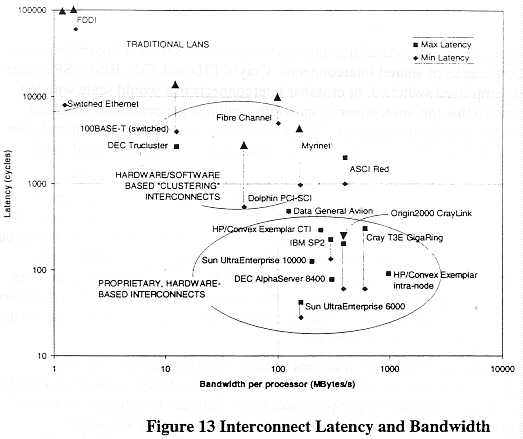
The chart shows that interconnects fall into three categories whose latency and bandwidth may differ from one to the next by an order of magnitude or more. The poorest performing interconnects are the traditional local area and wide area networks. Because they are designed to operate cheaply, span several hundred meters or even kilometers, and provide reliable data transport over unreliable media, these networks have extremely high protocol and operating system overhead. Data exchange may consume tens or hundreds of thousands of CPU cycles. Because the media are often shared, the per-processor bandwidth is very low.
At the other extreme are proprietary, in-box interconnects designed for the highest bandwidth and lowest latency feasible. Designed to function over very short distances in highly controlled environments, these interconnects exhibit very low overhead. Data exchange is managed entirely by the hardware. Designing and building such interconnects is very difficult, costly and requires highly specialized expertise and engineering ability.
Between these two extremes is a growing class of modest latency, moderate-to-high bandwidth interconnects. These hold a great deal of promise for aggregating multiple conventional workstations or servers into unified "clusters" whose aggregate performance can be applied to computational problems with much more efficiency than networked systems of the past. This class of interconnects, which emerged only in the middle of the 1990s, offers an excellent means of creating systems with modest levels of parallelism at modest cost using off-the-shelf technologies While they have substantially less overhead than networks, using the interconnects
35
requires a combination of hardware and software mechanisms that have so far prevented their achieving latencies as low as the proprietary interconnects. In fact, the gap between the clustering interconnects and the proprietary interconnects is somewhat greater than what is shown here The operating system and network protocols can increase the latencies by an order of magnitude or more Furthermore, traditional networking and today's clustering interconnects have much higher and less predictable variation in latency than do the proprietary interconnects. The latter are usually designed to provide uniform, or at least predictable latency with a well-known upper limit
Two clustering interconnect technologies in particular are noteworthy: Myrinet from Myricom, Inc., and the Scalable Coherent Interconnect embodied in products from a number of vendors. Myrinet [23] is a Gigabit-per-second packet-communication technology that can be used either as a local area network or as a "system area network" connecting components of a single configuration, often housed in the same rack. Components are connected to a switch by a single, non-shared link. What distinguishes the network is its low latency and high throughput, 160 Mbytes per port. In most networks, packets are sent across a link as a stream of bits. All bits that are part of a single packet are collected at an intermediate node before any bits are transmitted along to the next node. Myrinet employs "cut-through" routing in which the switch does not wait for an entire packet to arrive before transmitting the leading bits to their destination. The interconnect has round-trip latencies between approximately 10 and 200 microseconds, depending on the packet size and the control software used. At present, Myrinet switches are limited to eight ports. Switches may be linked to switches to expand the number of nodes, but the behavior of such combinations may not scale well for moderate or heavy loads, due in part to the blocking nature of the switch [24].
Another noteworthy development is the Scalable Coherent Interconnect (SCI). SCI is a 1992 ANSI/IEEE standard that describes an interconnect supporting a shared-memory model across memory that is physically distributed [25-27]. It acts like a processor/memory bus, but permits higher levels of parallelism than a shared bus, which can quickly become saturated. SCI is significant from both a networking perspective, and a systems architecture perspective (described below). From a networking perspective, SCI enjoys low latencies (a few microseconds) because it keeps data as ordinary variables stored at ordinary memory addresses. In contrast, networking protocols spend a great deal of time moving data from memory locations to buffers which are passed from the I/O system to the operating system to the user and back again. Numerous HPC vendors, including HP/Convex, Cray, Sun Microsystems, Data General, and Sequent have created, or commissioned, implementations for use in their own systems. Dolphin Interconnect Solutions is a leading vendor of SCI products.
Finally, it should be pointed out that the interconnect used in the SP2 is more closely related to the clustering interconnects than to the proprietary, hardware-oriented interconnects among which it is plotted in Figure 13. First, there is no hardware message-passing mechanism, so the hardware latency is unattainable. The minimum latency in practice is likely to be on the order of tens of microseconds [28]. Second, the Power microprocessors have much slower clocks than their competitors, so latency measured in clock cycles is lower in the SP2 than in other systems
36
with faster clocks At the same time, the SP high-speed switch is able to scale efficiently to much higher node counts than other clustering interconnects.
The classification of interconnects described above has a number of points of significance for The export control regime First, the decision not to compute an aggregate CTP for systems joined by a local area network is probably justified. While these traditional clusters may be very useful as throughput engines in which different serial processes are farmed out to run on single workstations, the poor performance of the interconnect makes it enormously difficult, if not impossible, to apply them all to a single application The performance gap between networks and proprietary interconnects is huge.
Second, there are significant differences between interconnects available today that impact real performance; however, these differences are not always reflected in the CTP metric In other words, eight Alpha workstations on a LAN are not equivalent to eight workstations connected via Myrinet, which are not equivalent to an eight-processor AlphaServer 8400 or a small configuration Cray T3E. Each system uses the same processor, but aggregations using poorer interconnects should not be viewed as equal substitutes for those using more sophisticated interconnects. Similarly, the presence of clusters in foreign countries should not, by itself, legitimize the export of systems with identical processors but more sophisticated interconnects.
In addition to differences in the performance of the interconnects, there are substantial differences in the software environments of clusters and integrated systems that make the former much more difficult to use in a production environment than the latter. What distinguishes, for example, the SP2 from a cluster of workstations? While the hardware is similar to that used in clusters, most of the value added by the SP lies in software. By far, the bulk of IBM's SP2 and RS/6000 SP development dollars have been spent on software. Creating a system that has the ability to concentrate the available hardware resources efficiently on a single problem across a broad spectrum of applications involves much more than connecting pieces of hardware. A great deal of specialized software is required to harness the CPU cycles efficiently, provide the necessary input/output and file management, make the system easy to monitor and manage, and ensure reliable operation over extended periods of time. In other words, creating a system with a great deal of capacity (total CPU cycles) is easy. Creating a system with high capability and good usability features is difficult, especially across a broad spectrum of applications.
While significant strides are being made towards developing the systems software necessary to effectively harness clusters, at present such efforts are, for the most part, still in the proof-of-concept stage. Where clusters are being used in a production capacity, the range of applications is limited. A recent NASA workshop addressed the opportunities and limitations of so-called Beowulf-class clusters. These are clusters using only mass-market commercial off-the-shelf components, freely available operating systems, and industry-standard software packages. The workshop determined that "Beowulf-class systems can deliver multi-Gflops performance at unprecedented price-performance but that software environments were not fully functional or robust, especially for larger 'dreadnought' scale systems [hundreds of processors]" [24].
Finally, the emerging "clustering interconnects" make parallel processing more accessible and affordable than ever before tO practitioners throughout the world. Clusters of workstations using
37
clustering interconnects have been used to run important applications characterized by high computation/communication ratios. They are likely to be a permanent feature on the international HPC landscape.
Trends in multiprocessor architectures
In the past, high-performance computing systems have been neatly divided into shared-memory multiprocessors with modest numbers of processors, and distributed-memory systems with a potentially large numbers of processors. The former offered programmers a familiar programming model with a single global memory space and uniform access times to all main memory locations. The latter supported much greater numbers of processors, but at the cost of a distributed memory programming model that forced applications programmers to play close attention to, and manage, the physical location of data throughout the system.
Distributed Shared Memory Architectures
One of the major architectural shifts in recent years has been towards a distributed shared memory (DSM) architecture in which memory is physically distributed, but logically shared. Like traditional distributed-memory architectures, DSM architectures accommodate larger numbers of processors than traditional shared memory architectures. Like traditional shared-memory architectures, however, the DSM architectures support the shared-memory programming model. Because of the physical distribution of memory, it is no longer possible to guarantee uniform access times to all memory locations. Consequently, such systems are frequently called Non-Uniform Memory Access (NUMA) systems.
In 1991, Kendall Square Research became the first company to offer commercial systems incorporating distributed shared memory. Convex introduced a physically distributed but globally shared memory in its Scalable Parallel Processor (SPP)-1000 in 1994. More recent adopters of this architecture include Data General (NUMAliiNE systems, 1995), Silicon Graphics (Origin2000, 1996), and Sequent Computer Systems (NUMA-Q, 1996).
Underlying each of these systems is a means of moving data among physically distributed memory locations, while maintaining the illusion of a single, shared memory space to the processors. If multiple copies of data elements are to be stored, then those copies must be kept consistent with each other. "Cache coherent" is a term frequently associated with NUMA architectures that refers to this consistency.
Kendall Square pioneered such a technology with its AIl,CACHE interconnect, and engineers at Dolphin Interconnect Solutions, Inc., acquired the intellectual property rights to ALLCACHE and further extended these and other ideas.
During 1990-1992, an IEEE standard, the Scalable Coherent Interconnect (SCI), was developed through a collaboration between individuals at National Semiconductor, Hewlett-Packard, Dolphin, MIPS Technology, MicroUnity Systems, the University of Wisconsin, and others [25]. In the years since its introduction, SCI has been implemented by a number of different vendors in a variety of capacities. Data General and Sequent employ SCI to build systems based on Intel
38
microprocessors that scale to 32 processors. Cray Research based its GigaRing on SCI technologies, although the Cray T3E does not support a global shared memory paradigm. Dolphin Interconnect has developed clustering technologies for Sun Microsystems that employ SCI. The SGI Origin2000 is not based on SCI, but rather a proprietary cache-coherent NUMA design.
In their current product lines, many HPC vendors have combined architectural features of the shared-memory SMP and distributed memory MPP architectures to create new systems based on physically distributed, logically shared memory systems employing crossbar or switched interconnects that scale well beyond the limits of traditional SMP platforms.
The strong emergence of DSM systems comes just at the time when practitioners using the most powerful systems have gained considerable experience using distributed memory programming models such as that supported by the Message Passing Interface (MPI). The role of MPI as a catalyst in facilitating the migration of codes to distributed memory systems is discussed in Chapter 4.
Hierarchical, Modular HPC
A second major trend in HPC architecture, often coupled with the trend toward DSM, is the grouping together of processors into multiprocessor modules with uniform access to locally shared memory, and combining these modules into larger systems which may employ a distributed- or NUMA- architecture between modules. Rather than build systems as a single tier of processors joined by a single interconnect, the hierarchical, modular design often employs one kind of interconnect to group together 4-16 processors into nodes, and another kind to aggregate the multiprocessor nodes.
The motivation for these kinds of architectures comes from two quarters. one approach is represented by HP/Convex's SPP and Exemplar systems and, more recently, IBM's RS/6000 SP. It is easier and cheaper to provide a given level of interconnect performance for a few processors than for many. At the same time, many applications have good data and instruction locality; that is, the data and instructions needed in the near future are likely to be located close to the instructions and data recently used. Designers can take advantage of these features to build systems in which a limited number of processors have fast and wide access to a portion of memory located nearby, and more limited access to memory further away.
HP/Convex's SPP and Exemplar systems use "hypernodes" of up to 16 processors which use a very high bandwidth and low latency crossbar interconnect to link these processors with shared memory. The Coherent Toroidal Interconnect (CTI) is based on SCI to connect the hypernodes with each other. With the introduction of its "high nodes" for the RS/6000 SP in 1996, IBM introduced a new architecture in which each node consisted not of a single processor, but of a symmetric multiprocessor (SMP) system with multiple processors joined by a shared bus to shared memory.
The alternative path to hierarchical, modular architectures comes from vendors of traditional SMP systems who wish to aggregate them into larger configurations beyond the limits of a
39
shared bus. Silicon Graphics' PowerChallenge Array epitomized this approach. The PCA consisted of multiple. shared-memory PowerChallenge SMPs connected by a switched interconnect into a distributed-memory cluster. Sun Microsystems is also offering clustering technologies to unite multiple SMP systems. In the lower-end markets, several companies are taking advantage of Intel's creation of so-called "Standard High Volume (SHV) servers," or "quads," which are single-board units consisting of four Pentium Pro processor linked by a 528 Mbytes/sec bus to shared main memory [22]. These four-processor units form basic building blocks, which can be combined in a number of ways to create larger shared or distributed memory configurations. Sequent, Data General, and NCR are among the companies actively pursuing this route. Each of these companies views its proprietary interconnect as part of the value it adds to systems development.
40
Table 3 summarizes the developments of various HPC vendors with respect to these trends.
| Vendor system | Year | Distributed Shared Memory | Hierarchical Modular Systems |
| IBM RS/6000 SP |
Various | Not supported | Nodes are SMP systems, currently up to 8-way, increasing to 32-way in the future. Nodes interact via a high-speed switch |
| SGI PowerChallenge Array |
1995 | Not supported | PowerChallenge XL SMPs clustered together via high-speed interconnect. Distributed memory outside of SMPs; shared memory within |
| SGI Origin2000 | 1996 | Employs Scalable Shared Memory Processing (S2MP). Shared memory up to 32 processors (mid-1997) increased to 64 and 128 during late 1997 and 1998. |
Smallest module is dual- processor board. Hierarchical modular architecture much less pronounced than in PowerChallenge Array |
| HP/Convex Exemplar |
1996 | Supported by Coherent Toroidal Interconnect (CTI) |
Hypernodes consist of 16-way SMP architecture. Multiple hypernodes connected by CTI |
| Sequent NUMA-Q |
1996 | Supports CC-NUMA architecture via IQ-Link, based on SCI |
Uses Intel SHV modules of four Pentium Pro processors linked via IQ-Link |
| Data General AViiON 2000 |
1996 | Uses the Synchronous Coherent Memory technology |
Uses Intel SHV modules |
| Cray T3E | 1996 | Uses a distributed memory programming model, although global memory addressing is supported. |
Not supported. Uses single tier architecture. Future generation of T3E to merge into Origin line. |
| Sun UltraEnterprise |
1996 | Not currently supported, although future developments likely to incorporate some related ideas. |
Clustering solutions join SMPs into a distributed memory, message-passing configuration. |
| DEC AlphaServer |
various | Not currently supported. Galaxies Software Architecture likely to offer some global perspective on memory, although not necessarily a shared memory programming model. |
Great emphasis on clustering SMP systems together using Trucluster or other technologies. Galaxies Software Architecture represents next stage of evolution of these technologies. |
Table 3 Current HPC Systems and Trends
41
Major Shifts in HPC Architectures?
What kinds of major shifts in system architecture can we expect over the next 3-5 years? There is little indication that architectures will change dramatically in the next half-decade. Both SGI/Cray and IBM have introduced new architectures since 1996. For them, developments in the coming years will be largely incremental. SGI/Cray is faced with the great technical challenge of integrating the SGI and Cray Research product families and overcoming current financial difficulties. IBM will expand the size of its nodes, but is unlikely to introduce a dramatically new architecture soon. It will take some time for software developers to learn to take full advantage of the several different kinds of memory available in the recent RS/6000 SP systems.
The leading candidates for new architectures are Sun Microsystems and DEC, each of which has gone for many years without introducing a new architecture. Both companies have released few details about their future plans. That which has been released would seem to indicate plans to "do the same thing only better" than their competition, rather than break new architectural ground.
Although the underlying architectures may not deviate dramatically from current ideas, we can expect, however, significant improvements in the ease and efficiency with which the power of large numbers of processors can be harnessed. The number of processors that fit in a given space is likely to increase. The HP V2200 and Sun UltraEnterprise 4000 are indicative of a trend that is likely to be repeated throughout the industry. These two systems pack over a dozen processors into a deskside chassis. In general, however, a good deal remains to be done in developing systems software that truly scales with the number of processors, offers distributed computing services, provides the user with a simple interface to the system, and has good performance for large configurations.
Implications for the Export Control Regime
This chapter has presented a sampling of some of the most significant trends in the HPC industry from the perspective of the export control regime. From them, a number of conclusions can be drawn:
42
References
[1] Gwennap, L., "PowerPC Team Outlines Future Plans," Microprocessor Report, Vol. 10, No. 11, Aug 26, 1996.
[2] Matzke, D., "Will Physical Scalability Sabotage Performance Gains?" IEEE Computer, Vol. 30, No. 9, Sep, 1997, pp. 37-39.
[3] Architects Look to Processors of Future, Microprocessor Report, Vol. 10, No. 10, Aug 5, 1996.
[4] Takahashi, D., "Chip Firms Face Technological Hurdles That May Curb Growth, Report Suggests," Wall Street Journal, Dec 1, 1997, p. B8.
43
[5] The National Technology Roadmap for Semiconductors. Semiconductor Industry Association, San Jose, CA, 1994.
[6] Burger, D. and J. R. Goodman, "Billion-Transistor Architectures," IEEE Computer, Vol. 30, No. 9, Sep, 1997, pp. 46-48.
[7] Patt, Y. N. et al, "One Billion Transistors, One Uniprocessor, One Chip," IEEE Computer, Vol 30, No. 9, Sep, 1997, pp. 51-57.
[8] Smith, J. E. and S. Vajapeyarn, "Trace Processors: Moving to Fourth-Generation Microarchitectures." IEEE Computer, Vol. 30, No. 9, Sep, 1997, pp. 68-74.
[9] Kozyrakis, C. E. et al, "Scalable Processors in the Billion-Transistor Era: IRAM," IEEE Computer, Vol. 30, No. 9, Sep, 1997, pp. 75-78.
[10] Hammond, L., B. A. Nayfeh, and K. Olukotun, "A Single-Chip Multiprocessor," IEEE Computer, Vol. 30, No. 9, Sep, 1997, pp. 79-85.
[11] Waingold, E. et al, "Baring it All to Software: Raw Machines," IEEE Computer, Vol. 30, No. 9, Sep, 1997, pp. 86-93.
[12] Lipasti, M. H. and J. P. Shen, "Superspeculative Microarchitecture for Beyond AD 2000," IEEE Computer, Vol. 30, No. 9, Sep, 1997, pp. 59-66.
[13] Gwennap, L., "Estimating IC Manufacturing Costs," Microprocessor Report, Vol. 7, No. 10. Aug 2, 1993.
[14] Smith, N. P., "Hits & Misses: Benchmarks Again, Fab Costs, and Jell-O," HPCWire, Nov 10, 1995 (Item 8060).
[15] Yu, A., "The Future of Microprocessors," IEEE Micro, Dec, 1996, pp. 46-53.
[16] Diefendoff, K. and P. K. Dubey, "How Multimedia Workloads Will Change Processor Design," IEEE Computer, Vol. 30, No. 9, Sep, 1997, pp. 43-45.
[17] Gwennap, L., "Multimedia Boom Affects CPU Design," Microprocessor Report, Vol. 10, No. 16, Dec 5, 1994.
[18] Gwennap, L., "UltraSPARC Adds Multimedia Instructions," Microprocessor Report, Vol. 8. No. 16, Dec 4, 1994.
[19] Gwennap, L., "Digital, MIPS Add Multimedia Extensions," Microprocessor Report, Vol. 10, No. 15, Nov 18, 1996.
44
[20] Wilson. R . "Sun s processor focuses on the problems of intense multiprocessing -- UltraSPARC-m targets servers, LAN switches," Electronics Engineering Times, No 974 Oct 6, 1997.
[21] Song, P., "UltraSparc-3 Aims at MP Servers," Microprocessor Report, Vol 11, No 14, Oct 27, 1997.
[22] Gwennap, L., "Intel's P6 Bus Designed for Multiprocessing," Microprocessor Report, Vol 9, No. 7, May 30, 1995, pp. 1-6.
[23] Myrinet. A Brief, Technical Overview, Myricom, Inc., http://www.myri.com/myrinet/overview.html, July 7, 1997.
[24] Sterling, T. et al, Findings of the first NASA workshop on Beowulf-class clustered computing, Oct. 22-23, 1997, Pasadena, CA, Preliminary Report, Nov. 11, 1997, Jet Propulsion Laboratory.
[25] Beck, A., "Dave Gustavson Answers Questions about SCI: Part I," HPCWire, Oct 4, 1996 (Item 10249).
[26] Beck, A., "Dave Gustavson Answers Questions about SCI: Part II," HPCWire, Oct 11, 1996 (Item 10282).
[27] Beck, A., "Dave Gustavson Answers Questions about SCI: Part III," HPCWire, Oct 18, 1996 (Item 10316).
[28] IBM Corp., The RS/6000 SP High-Performance Communication Network,
http://www.rs6000.ibm.com/resource/technology/spsw1/spswp1.book1.html.